Diamond-cooled chips could be the future
In order to significantly increase the performance of microprocessors despite enormous heat development, a US company is using diamonds for cooling. In experiments, one of the most powerful Nvidia chips calculates three times faster than was previously possible. The technology originally comes from Augsburg.
Moore's Law, according to which the computing power of computer chips doubles every two years, has not applied for some years now. This is mainly due to the fact that processors can no longer be cooled sufficiently if they were allowed to work as fast as they actually could. Neither the main processor (CPU) nor the graphics processor (GPU) can cope with much more than 100 degrees in the long term.
Scientists are therefore looking for alternative architectures. For example, TU Berlin and MIT Boston have achieved promising results with a prototype laser chip. Using light particles (photons) instead of electrons, it can work much more efficiently than conventional processors. However, it will still be a while before such systems are ready for series production. Alternatively, attempts are therefore being made to find methods of cooling conventional chips more effectively. One promising approach comes from a US company that uses diamonds for this purpose.

"World's largest diamond" from Augsburg
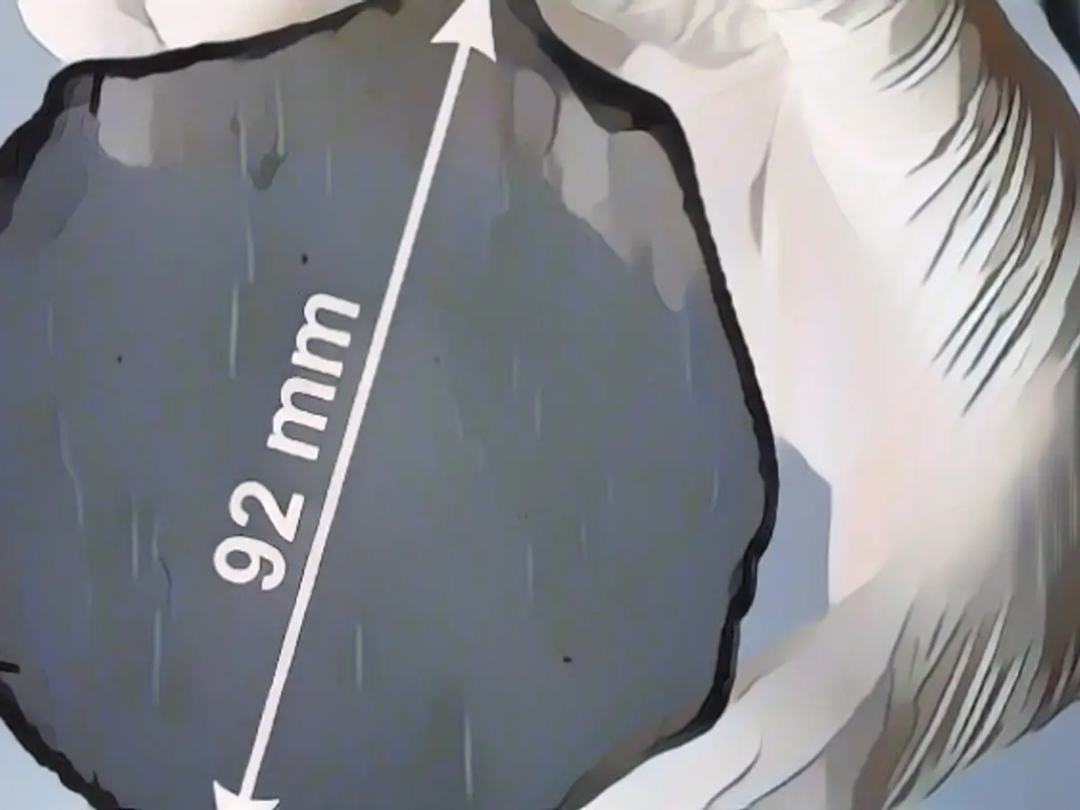
Strictly speaking, these are synthetic diamonds. Six and a half years ago, the University of Augsburg caused a stir when it grew the "world's largest diamond" in the laboratory. However, it did not resemble a real gemstone, as the 155-carat diamond was a disc with a diameter of 92 millimetres.
The shape is created as carbon molecules from a plasma at several thousand degrees are deposited layer by layer on an iridium base in a reactor at a negative pressure of a few tenths of an atmosphere. The Bavarian scientists knew early on that their wafers were "the ultimate material for high-performance electronics". They founded Augsburg Diamond Technology GmbH in 2015 to implement their findings commercially.
Double to triple the clock rate
Since last year, Audiatec has been owned by the US company Diamond Foundry, which is able to use the Swabian technology to produce diamond wafers less than three millimetres thick and 100 millimetres in diameter. With this material as cooling, chips could be operated at twice the otherwise possible clock rate without failures, CEO Martin Roscheisen told the"Wall Street Journal". In the case of one of Nvidia's most powerful chips, they were even able to triple the performance. Roscheisen is also German and is regarded as a star founder in Silicon Valley.

Diamond Foundry has already produced hundreds of diamond wafers. According to Roscheisen, his company is in talks with most of the world's largest chip manufacturers as well as defence companies and manufacturers of electric vehicles in order to speed up their microchips and electronics and minimize the space required. Diamond wafers are now as cheap as silicon carbide wafers, which are used to manufacture particularly efficient power semiconductors.
There is another way
However, Roscheisen's company is not without competition, writes the Wall Street Journal. There are companies that can produce even larger synthetic diamonds using other processes. There are also other approaches. Intel, for example, is working on placing microchips on a glass back.
This makes it possible to produce mega-chips, which in principle are made up of many small chips (chiplets). These remain stable with high power consumption and the associated heat development. The heat output per package is up to one kilowatt, Intel fellow Rahul Manepalli told the Wall Street Journal. A chip package measures ten square centimeters and absorbs about the power of a hair dryer.
Boron arsenide could be an alternative to silicon in the future. Although it does not conduct heat quite as well as diamonds, it is also a semiconductor. Extremely powerful microchips could therefore be produced from this material.
Andy Bechtolsheim, co-founder of Sun Microsystem, can also imagine a combination of different technologies in a sandwich structure. "Glass on top for fast communication, a three-dimensional stack of silicon layers in the middle for processing and a diamond wafer at the bottom to dissipate all the heat," he told the Wall Street Journal.
The US company is utilizing synthetic diamonds, grown by Augsburg University six and a half years ago, to enhance the cooling capacity of their computer chips, allowing for a threefold increase in performance for one of Nvidia's most powerful chips.
With their ability to produce diamond wafers less than three millimeters thick, Diamond Foundry, now the owner of Audiatec, enables chips to operate at clock rates double the usual limit without failures, resulting in a tripled performance for certain Nvidia chips.
Source: www.ntv.de


